Custom Sensor Telemetry Board
Custom 4-layer STM32F411 PCB with FreeRTOS environmental telemetry
View repositoryMCU
STM32F411RET6 (LQFP-64)
Board
4-layer · 51.2 × 40 mm
Sensor
BME280 + SSD1306 @ 400 kHz
Link
UART 921600 baud · USB-C
01Overview
An end-to-end embedded product spanning schematic capture, PCB layout, manufacturing, and firmware. The board integrates an STM32F411RET6 microcontroller, a Bosch BME280 environmental sensor and a 128×64 SSD1306 OLED sharing a single 400 kHz I²C bus, and USB-C connectivity through a CP2102N UART-to-USB bridge, all on a compact 4-layer board prepared for JLCPCB PCBA.
The goal was to own the full hardware-to-firmware stack: design the electronics, get the board manufactured, bring it up on the bench, and write the FreeRTOS firmware that turns raw sensor reads into a reliable telemetry stream.
02Problem Statement
Off-the-shelf dev boards hide the engineering that matters in embedded work: power sequencing, decoupling, bus layout, and bring-up. Building a custom board surfaces all of it.
The system needs to sample environmental data continuously while transmitting telemetry without dropping samples or corrupting the shared buffer. That is a concurrency problem that maps naturally onto an RTOS.
03Architecture
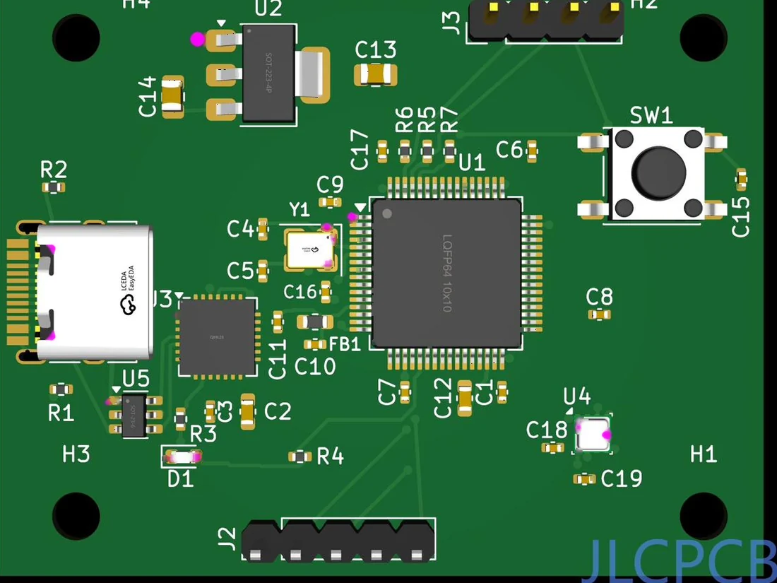
Hardware: STM32F411RET6 in an LQFP-64 package is the controller, clocked from an 8 MHz crystal through the PLL to 100 MHz. An AMS1117 3.3 V LDO with decoupling supplies the MCU and peripherals, and a USBLC6-2 protects the USB data lines. The BME280 at I²C address 0x77 and an SSD1306 OLED at 0x3C share the bus; a CP2102N bridges the MCU's UART to a USB-C connector for host telemetry and power. An SWD debug header exposes the core for flashing and live debugging.
Firmware: bare-metal C with no HAL, configuring the chip through CMSIS registers directly, running under FreeRTOS. Four tasks run concurrently: sensor_task reads and Bosch-compensates the BME280, telemetry_task frames each sample with a CRC-16/CCITT checksum and sends it over UART at 921600 baud, display_task renders pages to the SSD1306, and heartbeat_task blinks the status LED and kicks the independent watchdog. A queue carries samples between acquisition and telemetry, and an I²C mutex arbitrates the shared bus so the two peripherals never collide mid-transaction.
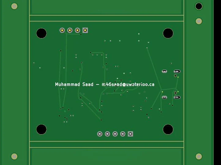
Layout: the 4-layer stackup on 1.6 mm FR4 gives the two inner layers to a solid ground plane and a +3V3 plane, leaving both outer layers for signals. The I²C bus is kept short with decoupling placed close to the supply pins.
04Technical Challenges
Manufacturability and DFM
Getting the design manufacturable was the core hardware challenge. The layout tripped a via-in-pad DFM flag, resolved by specifying plated-over filled vias, epoxy-filled and copper-capped, so the pads stay solderable. The design is DFM-validated with POFV across all vias and the board is in fabrication ahead of bench bring-up.
I²C bus integrity at 400 kHz
Running the BME280 at I²C Fast Mode (400 kHz) requires a clean bus: short traces, correct pull-ups, and careful placement. Bus layout was treated as a first-class signal-integrity concern rather than an afterthought.
Lossless concurrent telemetry
Acquisition and transmission run concurrently, so the shared sample buffer is a contention point. A mutex guards it to guarantee that the telemetry task never reads a partially-written sample.
05Implementation Details
Schematic and 4-layer layout in KiCad
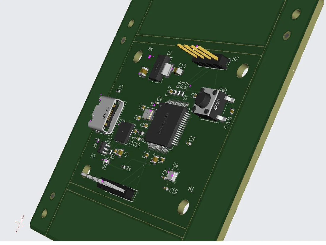
Designed the full schematic and a 4-layer, 51.2 × 40 mm board in KiCad: STM32F411RET6 (LQFP-64), BME280 over I²C, CP2102N USB-C bridge, 3.3 V LDO with decoupling, and an SWD header. Components were selected and signal paths routed with power integrity and I²C bus layout as explicit constraints.
Manufacturing and assembly
Gerbers, BOM, and centroid files are generated from the KiCad project for a JLCPCB PCBA order. The design cleared DFM review after the via-in-pad flag was resolved with plated-over filled vias; the board is in fabrication, with bench bring-up to follow.
FreeRTOS firmware in C
Firmware is bare-metal C on the STM32F411RET6 with no HAL, configuring the RCC clock tree, GPIO, I²C, UART, and EXTI through CMSIS registers directly. Four FreeRTOS tasks handle acquisition, CRC-framed telemetry, OLED rendering, and a watchdog heartbeat, with a button on EXTI0 cycling display pages from its ISR. I²C runs at 400 kHz; UART telemetry runs at 921600 baud.
Timing validation
Bus and link timing were validated on a NUCLEO-F411RE with a logic analyzer, confirming the I²C transactions and UART framing against the datasheet ahead of custom-board bring-up.
06Key Engineering Decisions
Custom board over a dev kit
Designing a custom 4-layer board, rather than wiring a dev kit, was a deliberate choice to own power design, decoupling, and bus layout end to end, which is exactly the skill set embedded roles screen for.
FreeRTOS for concurrency
Acquisition and transmission are naturally concurrent with different timing needs, so an RTOS with mutex-protected sharing is a cleaner, more scalable model than a hand-rolled superloop.
CP2102N + USB-C for the host link
A dedicated UART-to-USB bridge keeps the host interface simple and robust while freeing the MCU to focus on acquisition, and USB-C gives a modern, reversible connector for power and data.
07Future Improvements
- Add DMA-driven I²C and UART to offload the CPU during transfers.
- Bring up the fabricated board on the bench and validate the telemetry chain end to end.
- Extend the host-side visualizer with logging and historical charting.
- Characterize current draw and add low-power sleep states between samples.
08Media & Documentation
Visual documentation for this project. Board views are exported from the KiCad project and the JLCPCB assembly preview; the remaining placeholder is reserved for a bench capture after bring-up.
Open to opportunities
Looking for a Summer 2027 internship.
If you're hiring for embedded, firmware, or hardware roles, I'd be glad to talk through my projects and how I work. The fastest way to reach me is email.